Breaking Barriers in Neuromorphic Computing with Ultra-Fast, Event-Driven Intelligence
- Pioneering Photonic Innovation: This breakthrough introduces the first silicon-compatible photonic spiking neural network (PSNN) chip, featuring gigahertz-scale spiking dynamics, in-situ training, and retina-inspired encoding to emulate brain-like asynchronous processing.
- Superior Performance and Efficiency: Achieving 80% accuracy on the KTH video recognition dataset, the chip processes data 100 times faster than traditional frame-based methods, overcoming electronics’ speed and energy limitations through photonic advantages like parallelism and low latency.
- Transformative Applications: By enabling real-time dynamic vision and adaptive decision-making, this technology paves the way for advancements in autonomous vehicles, robotic navigation, and beyond, signaling a shift from von Neumann architectures to neuroscience-inspired computing.
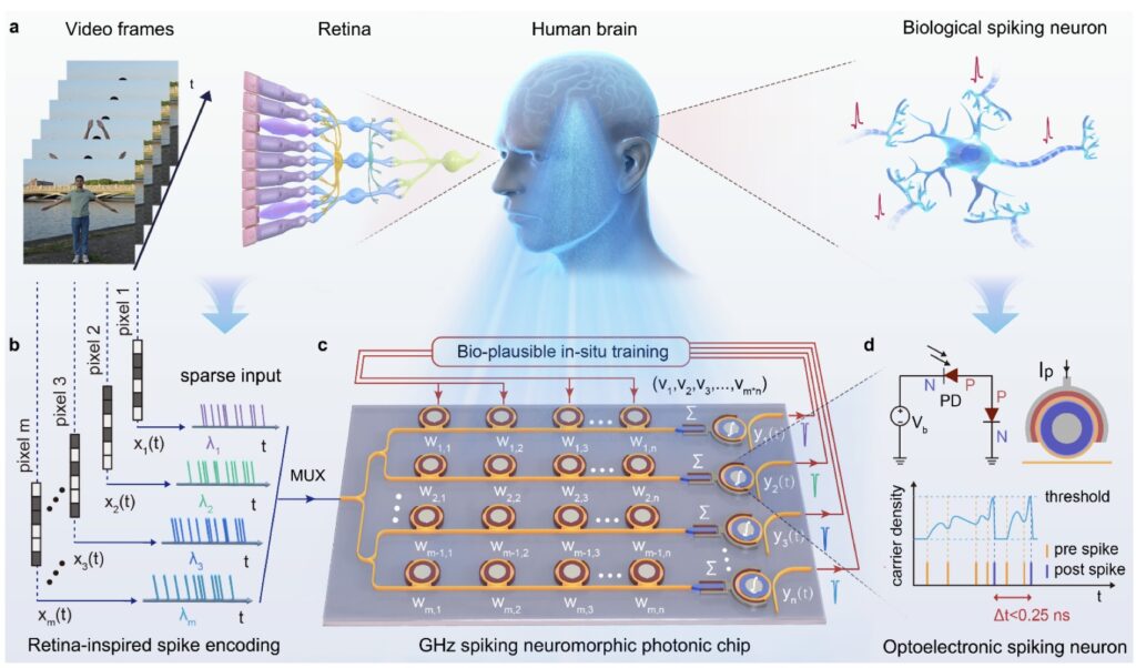
In the ever-evolving landscape of artificial intelligence, where the demand for faster, more efficient computing power seems insatiable, a groundbreaking development is poised to redefine the field. Enter the GHz spiking neuromorphic photonic chip—a marvel of engineering that bridges the gap between silicon technology and the intricate workings of the human brain. Inspired by neuroscience, neuromorphic computing doesn’t just simulate neural networks on traditional digital hardware; it emulates them at the hardware level, promising to shatter the bottlenecks of the von Neumann architecture. This chip, the first of its kind on a complementary metal-oxide-semiconductor (CMOS)-compatible silicon platform, represents a paradigm shift toward event-driven, asynchronous dynamics that have long eluded even the most advanced AI systems.
At its core, the photonic spiking neural network (PSNN) chip addresses critical shortcomings in current neuromorphic platforms. Electronic systems like IBM’s TrueNorth and the more recent Tianjic have made strides in energy efficiency through spike-based processing, but they grapple with inherent limitations as Moore’s Law slows and Dennard scaling ends. Electronics struggle with speed, bandwidth, and crosstalk issues, especially in handling dynamic, spatiotemporal data. Photonics, however, flips the script with its intrinsic parallelism, ultra-wide bandwidth, and near-zero latency. This chip leverages these strengths to create a full-stack, brain-inspired system that integrates gigahertz-scale nonlinear spiking dynamics, in-situ learning via supervised synaptic plasticity, and informative event representations through retina-inspired spike encoding. The result? A platform that resolves long-standing challenges in integrating and processing spatiotemporal information with remarkable energy efficiency.
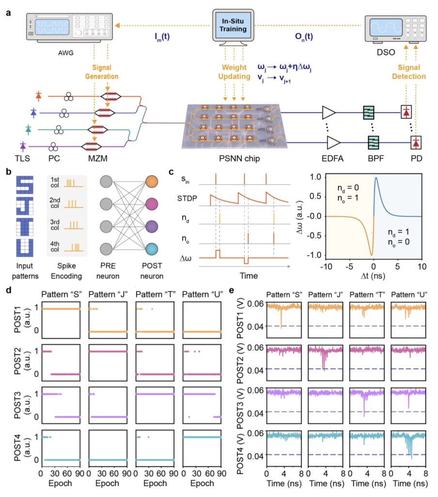
Diving deeper into the chip’s architecture, the key component is the micro-ring modulator (MRM) spiking neuron, characterized through a sophisticated experimental setup. Grating couplers interface single-mode fibers with bus waveguides, achieving an optimized coupling loss of about 7 dB per facet at 1550 nm. Pump light from a continuous-wave tunable laser is polarized and fed into the chip, while perturbation light is modulated using a high-speed Mach-Zehnder interferometer (MZI) intensity modulator operating at 25 GHz. This light is converted to a current signal via a photodetector and applied to the MRM through an RF probe. Electrical signals, generated by an arbitrary waveform generator (AWG) at 65 GSa/s and amplified to 55 GHz, drive the system. The output is amplified with an erbium-doped fiber amplifier (EDFA), filtered, detected, and captured on a high-speed digital oscilloscope. Communication between devices occurs via LAN cables on a standard desktop setup. By pumping the MRM in its excitable regime and applying perturbation pulses of varying strengths and durations, researchers have demonstrated neuron-like spiking dynamics that mimic biological excitability, paving the way for ultra-fast, event-driven computation.
Complementing the neurons is the micro-ring resonator (MRR) synapse array, a tunable weight bank that enables synaptic plasticity. The ten resonance wavelengths are thermally tuned for equal channel spacing by applying voltages from 0 to 3.6 V. A “weight-voltage” lookup table is created for each channel by sweeping voltages while keeping others constant, with pump wavelengths set precisely—such as 1550.170 nm for the first channel and 1557.370 nm for the last. For any given weight matrix, initial voltages are determined from these tables, followed by in-situ calibration to mitigate inter-channel thermal crosstalk. This setup allows for fine-tuned synaptic weights, essential for the chip’s learning capabilities. In pattern recognition tasks, a four-channel tunable laser operates at wavelengths like 1550.170 nm to 1552.570 nm. Input patterns, such as 5×4 binary pixel matrices, are temporally encoded into spike trains fed to pre-synaptic (PRE) neurons. Each black pixel becomes a 0.1 ns rectangular pulse, timed by a formula incorporating subscript indices and a 0.35 ns duration between representations. A padding sequence of three 0.4 ns pulses marks the start of each training epoch. The multiplexed signals are weighted by the MRR bank, converted to photocurrent, and applied to the MRM neuron, with attenuators and delay lines balancing power and timing across paths.
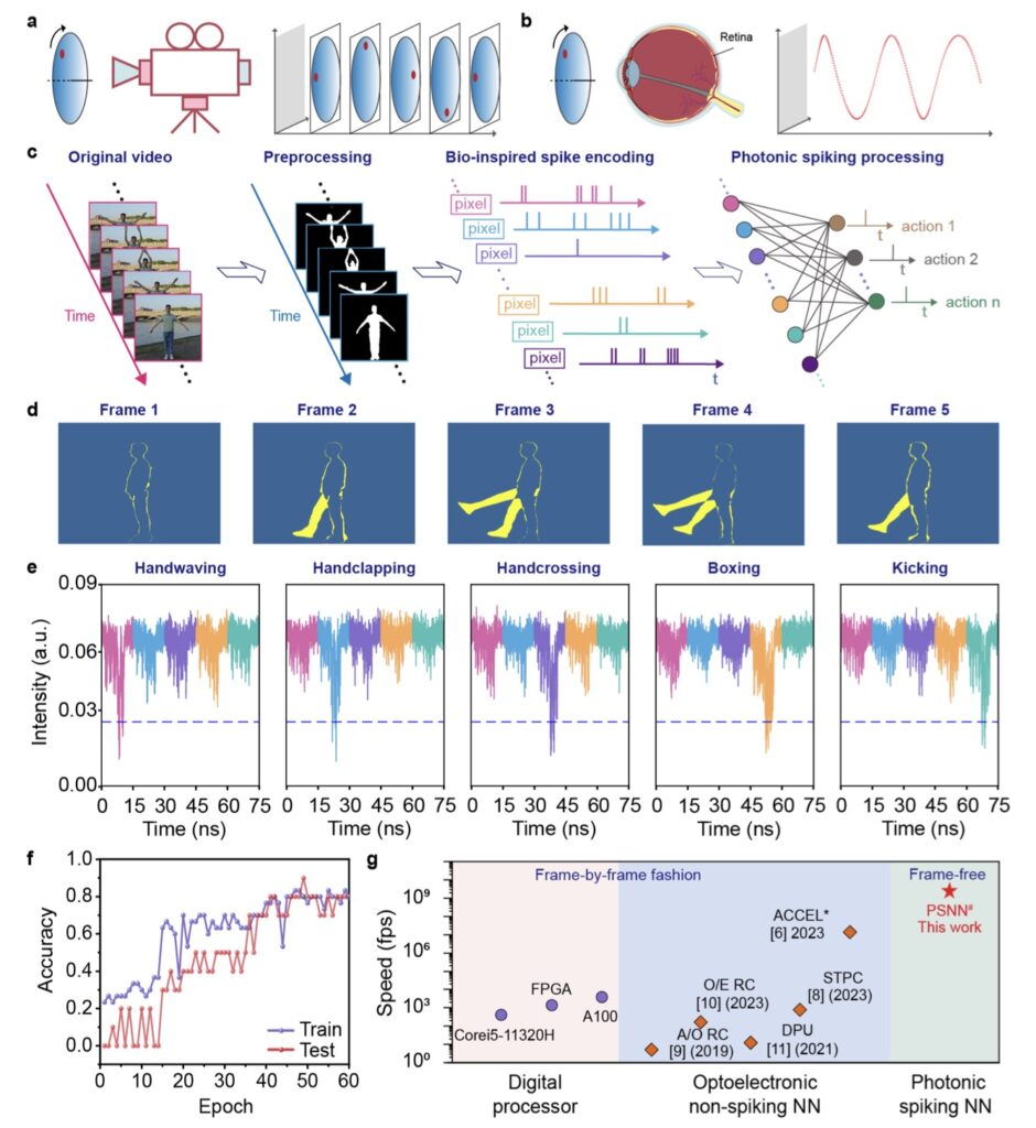
The chip’s prowess shines in real-world applications, particularly human action video recognition on datasets like KTH. Here, weighted-and-summed spike trains from input videos are converted into time-multiplexed AWG sequences and applied to an MRM neuron, which emulates post-synaptic neurons in sequence. This hardware-friendly approach has powered various applications, encoding pixel value changes between frames as 0.15 ns pulses within 0.28 ns windows, resulting in 10.92 ns spike trains per pixel over 39 time steps. Operating in a frame-free, event-driven manner, the system achieves 80% accuracy while running approximately 100 times faster than conventional frame-based methods. This efficiency stems from its spike-driven processing, ideal for dynamic spatiotemporal data, contrasting with computer-science-oriented photonic systems that merely emulate connectivity without true biological plausibility.
Looking broader, this PSNN chip isn’t just a technical feat—it’s a leap toward scalable neuromorphic computing with low latency and high throughput. By collocating memory and computation, employing event-based coding, and enabling synaptic plasticity, it mirrors the brain’s asynchronous efficiency more closely than ever. While electronic neuromorphics have advanced energy efficiency, photonics overcomes their physical constraints, opening doors to ultra-fast image classification, video recognition, and even artificial content generation. Yet, PSNN development is still nascent, with this chip marking a milestone in neuroscience-oriented photonics.
The implications are profound for fields demanding real-time processing, such as autonomous vehicles that need instant dynamic vision for obstacle avoidance or robotic navigation in unpredictable environments. Imagine drones adapting to changing weather on the fly or smart surveillance systems detecting anomalies in video streams without draining power. As we push beyond the end of Moore’s Law, this photonic innovation signals a future where AI isn’t just smart—it’s instinctively responsive, energy-thrifty, and blazingly fast. With continued refinements, from optimizing grating couplers to expanding synapse arrays, the GHz spiking neuromorphic photonic chip could very well be the cornerstone of next-generation machine intelligence, blending the best of biology and technology into a seamless, revolutionary whole.